Frequently asked questions
General questions about Raman Spectrometers
The term Raman spectrometer can have different meanings depending on the context. At Ibsen we identify a Raman spectrometer as a device that detects the spectrum from Raman scattered light. As such, it is a sub-part of a complete Raman spectroscopy instrument. However, you may also find the term Raman spectrometer used for the complete instrument.
A Raman spectroscopy instrument is a device that use the Stokes or anti-stokes wavenumber shift caused by Raman scattering to identify and/or quantity materials.
The key components of a Raman spectroscopy instrument are: a laser, a probe, a spectrometer, and a software model.
A Raman spectrometer typically consists of an entrance slit followed by collimating optics, a diffraction grating, focusing optics and a photo-detector array.
A Raman spectrometer uses a diffraction grating to separate the different wavelength components of the Raman spectrum angularly. The different wavelengths are focused on a linear photo-detector array which converts the light intensity at each wavelength to a voltage/current. A Raman spectrometer will include a narrow aperture (slit) at the entrance which determine the resolution of the spectrometer.
General questions about OCT Spectrometers
An OCT (Optical Coherence Tomography) spectrometer is an optical device used to measure the intensity of light across different wavelengths. It is used in OCT systems to generate detailed cross-sectional images of biological tissues.
OCT spectrometers are widely used in medical imaging, particularly in ophthalmology for retinal scans, as well as in cardiology, dermatology, and oncology. They are also used in industrial inspection, material science, and research.
Key factors include spectral range, resolution, sensitivity, roll-off, form factor, data interface options, and the specific requirements of your application such as the type of tissue or material you are analyzing.
An OCT spectrometer measures the interference pattern of light reflected from different depths within a sample. This data is processed to create high-resolution cross-sectional images, revealing detailed internal structures.
Roll-off refers to the decrease in sensitivity and signal strength as the depth of the sample increases. Minimizing roll-off is important for maintaining image quality at greater depths.
Yes, OCT spectrometers can be fully customized or adapted to meet the specific needs of different applications. This includes adjustments in spectral range, resolution, and form factor.
Common data interfaces include MIPI, USB, and CameraLink. The choice of interface depends on the desired data transfer speed and the compatibility with existing systems.
Yes, Ibsen Photonics offers standard OEM spectrometers with various configurations and data interfaces to suit different applications. These spectrometers offer a balance of performance and cost-effectiveness.
General questions about LIBS Spectrometers
A LIBS (Laser Induced Breakdown Spectroscopy) spectrometer is an analytical device that measures the light emitted from a plasma created by a laser pulse. This light emission is used to determine the atomic composition of the sample.
LIBS spectrometers are used in various fields such as materials science, metallurgy, environmental monitoring, pharmaceuticals, forensics, and geology. They are also widely used for quality control in manufacturing and industrial processes. Our LIBS spectrometers are extensively used in metal and mineral analysis for material characterization and quality control of raw materials.
A LIBS spectrometer works by firing a high-energy laser pulse at the sample, creating a plasma. The emitted light from this plasma is then analyzed by the spectrometer to identify the elements present in the sample.
Advantages include rapid and real-time analysis, minimal sample preparation, the ability to analyze solid, liquid, and gaseous samples, and the capability to detect a wide range of elements simultaneously.
The required spectral range for a LIBS spectrometer largely depends on the atomic elements that needs to be identified. Atomic transitions range from the UV through the NIR.
Key factors include sensitivity, resolution, spectral range, and synchronization between laser and spectrometer as well as environmental stability.
Yes, LIBS spectrometers can be customized to meet the specific needs of different applications, including adjustments in spectral range, resolution, and form factor.
Common data interfaces include USB and SPI. The choice of interface depends on the desired data transfer speed and compatibility with existing systems.
General questions about UV Spectrometers
A UV spectrometer is an instrument used to measure the intensity of light in the ultraviolet range (175-400 nm) of the electromagnetic spectrum. It analyzes how light interacts with a sample, providing valuable data for various applications.
Please note, that in some contexts a UV spectrophotometer denotes a spectrometer that covers both the UV and visible wavelength ranges.
UV spectrometers utilize a diffraction grating to disperse the spectrum across a photo-detector array
UV spectrometers are versatile tools used in many different applications like fluorescence and absorbance spectroscopy as well as Laser Induced Breakdown Spectroscopy.
When selecting a UV spectrometer, consider your requirements to wavelength range, resolution, sensitivity, and signal-to-noise ratio as key factors. Also, footprint, environmental robustness and cost should be considered.
Yes, our UV spectrometers are designed as OEM modules for seamless integration into your systems. Their compact design and advanced electronics ensure easy incorporation into various setups. Thanks to their modular spectrometer design, our solutions can be tailored to meet application-specific requirements across multiple industries.
OEM UV spectrometers offer high sensitivity and resolution, compact design, and robust construction. They provide accurate measurements and are suitable for both laboratory and field applications, enhancing your system’s capabilities. For OEM customers, we offer custom spectrometer solutions that integrate seamlessly into larger analytical systems and instruments.
General questions about UV-VIS Spectrometers
A UV-VIS spectrometer is an instrument used to measure the intensity of light from the ultraviolet to the visible range and sometimes also into the near infrared range of the electromagnetic spectrum. It analyzes how light interacts with a sample, providing valuable data for various applications.
Please note, that in some contexts a UV-VIS spectrometer is sometimes called a UV spectrophotometer or UV detector.
UV-VIS spectrometers utilize a diffraction grating to disperse the spectrum across an array of photo-detectors
UV-VIS spectrometers are versatile tools used in many different applications. Some of the more common applications are as UV-detector in HPLC systems and thin film measurements of coatings.
When selecting a UV-VIS spectrometer, consider your requirements to wavelength range, resolution, sensitivity, and signal-to-noise ratio as key factors. Also, footprint, environmental robustness and cost should be considered.
Yes, our UV-VIS spectrometers are designed as compact OEM modules ideal for seamless integration into your systems. Their compact design and advanced electronics ensure easy incorporation into various setups.
OEM UV-VIS spectrometers offer high sensitivity and resolution, compact design, and robust construction. They provide accurate measurements and are suitable for both laboratory and field applications, enhancing your system’s capabilities.
General questions about VIS Spectrometers
A VIS spectrometer is an instrument used to measure the intensity of light in the visible range (400-700 nm) of the electromagnetic spectrum. It can be used to analyze how light interacts with a sample, providing valuable data for various applications.
VIS spectrometers utilize a diffraction grating to disperse the spectrum across an array of photo-detectors.
VIS spectrometers are versatile tools used in many very different applications like color analysis, light source characterization, fluorescence and absorbance spectroscopy.
When selecting a VIS spectrometer, consider your requirements to wavelength range, resolution, sensitivity, and signal-to-noise ratio as key factors. Also, footprint, environmental robustness and cost should be considered.
Yes, our VIS spectrometers are designed as OEM modules for seamless integration into your systems. Their compact design and advanced electronics ensure easy incorporation into various setups.
OEM VIS spectrometers offer high sensitivity and resolution, compact design, and robust construction. They provide accurate measurements and are suitable for both laboratory and field applications, enhancing your system’s capabilities.
General questions about VIS-NIR Spectrometers
A VIS-NIR spectrometer is an instrument used to measure the intensity of light in the visible (VIS) range to near infrared (NIR) range (500-1100 nm) of the electromagnetic spectrum. It analyzes how light interacts with a sample, providing valuable data for various applications.
VIS-NIR spectrometers utilize a diffraction grating to disperse the spectrum across an array of photo-detectors
VIS-NIR spectrometers are versatile tools used in many very different applications like fluorescence and absorbance spectroscopy.
When selecting a VIS-NIR spectrometer, consider your requirements to wavelength range, resolution, sensitivity, and signal-to-noise ratio as key factors. Also, footprint, environmental robustness and cost should be considered.
Yes, our VIS-NIR spectrometers are designed as OEM modules for seamless integration into your systems. Their compact design and advanced electronics ensure easy incorporation into various setups.
Our OEM VIS-NIR spectrometers offer high sensitivity and resolution, compact design, and robust construction. They provide accurate measurements and are suitable for both laboratory and field applications, enhancing your system’s capabilities.
General questions about NIR Spectrometers
A NIR spectrometer is an instrument used to measure the intensity of light in the near infrared (NIR) range (900-2100 nm) of the electromagnetic spectrum. It analyzes how light interacts with a sample, providing valuable data for various applications.
NIR spectrometers utilize a diffraction grating to disperse the spectrum across an array of photo-detectors
NIR spectrometers have a wide range of applications across various fields due to its ability to analyze chemical and physical properties in solids and liquids. Some of the main applications are food and agriculture, phamaceuticals, environmental monitoring and chemical industry.
When selecting a NIR spectrometer, consider your requirements to wavelength range, resolution, sensitivity, and signal-to-noise ratio as key factors. Also, footprint, environmental robustness and cost should be considered.
Yes, our NIR spectrometers are designed as OEM modules for seamless integration into your systems. Their compact design and advanced electronics ensure easy incorporation into various setups.
Our OEM NIR spectrometers offer high sensitivity and resolution, compact design, and robust construction. They provide accurate measurements and are suitable for both laboratory and field applications, enhancing your system’s capabilities.
General questions about Gratings
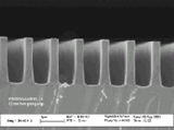
Ibsen fused silica transmission gratings are gratings that are structured directly into the surface of a fused silica substrate and comprise no other materials than fused silica. They are essentially a binary structure that is monolithically attached to the fused silica substrate. A SEM picture example of a typical grating is shown here:
We pattern our gratings by 2-beam interferometry (also known as holographically) or lithographically, initially into photoresist, which is then used as an etch mask to transfer the grating pattern into the fused silica by Reactive Ion Etching (RIE). Every grating is thus a high fidelity, high integrity master, not a replica.
Grating equation:
m · λ = Λ · (sin θI + sin θD)
where:
m is the m’th diffraction order
λ is the wavelength of the illumination
Λ is the grating period
θI is the incidence angle of the illumination
θD is the diffraction angle of the illumination for the m’th diffraction order,
with respect to the following schematic:
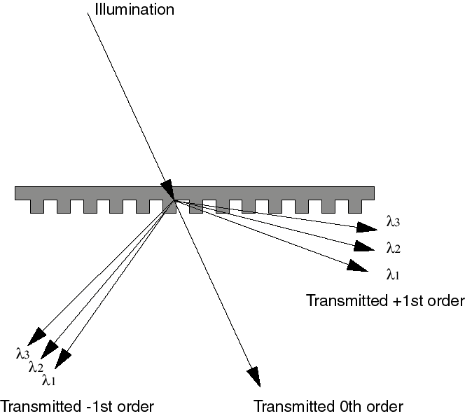
Reflection gratings are typically composed of a substrate material (typically a glass), an epoxy or photoresist into which the grating is profiled, and finally a metallic coating on top. All grating types can be made most efficient when optimized for Littrow (Bragg) angle of incidence, which for reflection gratings means that the light is retro-reflected, while transmission gratings have the output separated from the input. Thus, reflection gratings are most convenient when retro-reflection is desired (such as laser cavity feedback), whereas transmission gratings are most convenient for most other applications (such as spectroscopy, pulse compression and transmission optical devises.)
Transmission optics in general, and transmission gratings in particular, are much easier to align that their reflective counterparts. The following technical note explains why this is the case: Why are transmission gratings less angle sensitive than reflection gratings?
Surface relief, fused silica transmission gratings are monolithically integrated into the fused silica substrate surface, and thermally and environmentally just as stable as the blank fused silica substrate. VPH gratings are recorded into a gelatin material, sandwiched between 2 substrates with the edges sealed, as the gelatin material is environmentally instable. The temperature handling capability of gelatin-based VPH gratings is little more than 100 degrees C, while fused silica transmission gratings can withstand over 1000 degrees C.
The diffraction efficiency of surface relief gratings is 3 times less sensitive to angle of incidence variation than thick VPH gratings. This is fundamental (can be derived from Kogelnik’s original grating analysis work), and related to the refractive index modulation of the gratings – see for example “Dielectric surface-relief gratings with high diffraction efficiency” by Kiyoshi Yokomori, Applied Optics / Vol. 23, No. 14 / 15 July 1984.
For a narrow bandwidth, fused silica transmission gratings can be designed to theoretically have over 99% efficiency, for a single (TE-(s) or TM(p)) polarization, or even for both polarizations simultaneously. For more broad bandwidths there is a tradeoff between the spectral width and both the average and peak efficiency that can be achieved. For grating with bandwidths of an octave ( i.e. where the end wavelength is double the start wavelength) or more, fused silica transmission gratings can typically have 75% average efficiency. Narrowband gratings (up to half an octave) can typically have 90% average efficiency or more.
While the micro-structured grating surface should not be physically touched, the fused silica-based grating structure can handle most chemical cleaning. Bath-based cleaning processes can be established for a simple acetone – IPA – DI water clean, but the gratings can also handle detergent, moderate ultrasound, acid or alkaline chemicals.
For periodic cleaning requirements in the laboratory. We recommend the commercial cleaning solution called “First Contact”. This cleaning product is effective for many optics cleaning requirements. For further information on First Contact, please see the manufacturer’s web-site: http://photoniccleaning.com.
Transmission optics in general, and transmission gratings in particular, are much easier to align that their reflective counterparts. The following technical note explains why this is the case: Why are transmission gratings less angle sensitive than reflection gratings?
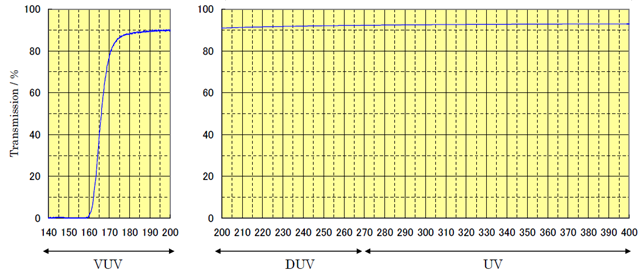
We make gratings for the entire transmission range of fused silica, which starts below 200 nm and goes beyond 2000 nm. The plot below show the UV applicability of UV grade fused silica material (and thus UV fused silica transmission gratings) – here shown as the external transmission (i.e. there is approx. 8% surface Fresnel reflection loss) of a 6.35 mm thick substrate.
Fused silica transmission gratings can handle just as much power and energy as blank fused silica substrates. Quantitative values depend on wavelength and pulse length. For CW illumination our gratings have been used at more than 400 kW/cm2, while with fs lasers our gratings have been used at more than 20 TW/cm2. Click here for more information about high power gratings.
We utilize holographic stepper and lithography stepper based production equipment for cost-effective, high volume production of gratings with sizes up to approx. 50 mm x 50 mm, and we are able to fabricate grating sizes up to 100-120 mm dimensions.
Fused silica transmission gratings can handle over 1000 degrees C. The CTE of fused silica is very low (0.5×10⁻⁶/°C) so the grating period is very insensitive to temperature change. Furthermore, as the change of the refractive index of fused silica with temperature also is very low (1.28×10⁻⁵/°C at 20 degrees C), the diffraction efficiency variation with respect to temperature is also negligible.
You can read more in our white paper on fused silica transmission gratings: White-paper-Fused-Silica-Transmission-Gratings
Want to know more?
For further information see below.
Ask the experts
Do you want to discuss your spectrometer project with one of our experts? Please fill out the form, and we will contact you as soon as possible.
Visit our OEM spectrometer pages
Browse our range of OEM spectrometer products.


